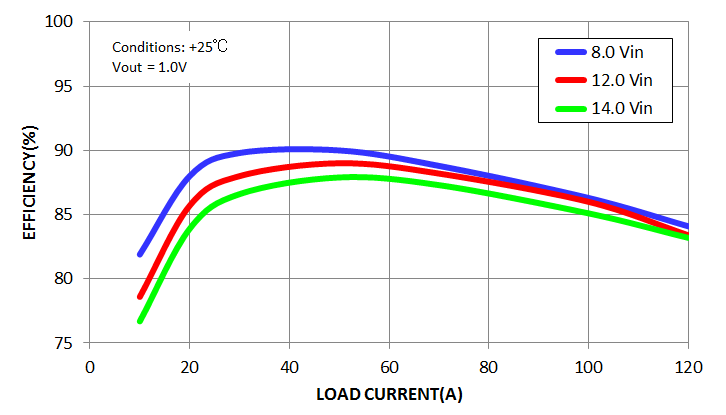
By the adoption of advanced high efficiency devices, high efficiency can be realized.
As equipment becomes more functional, high-end devices such as FPGA and ASSP consume more current, even a few percent difference in efficiency can result in a large loss of several watts.
By using a high-efficiency converter to reduce losses, it can contribute to energy saving and the reduction of components such as heat sinks and cooling fans.
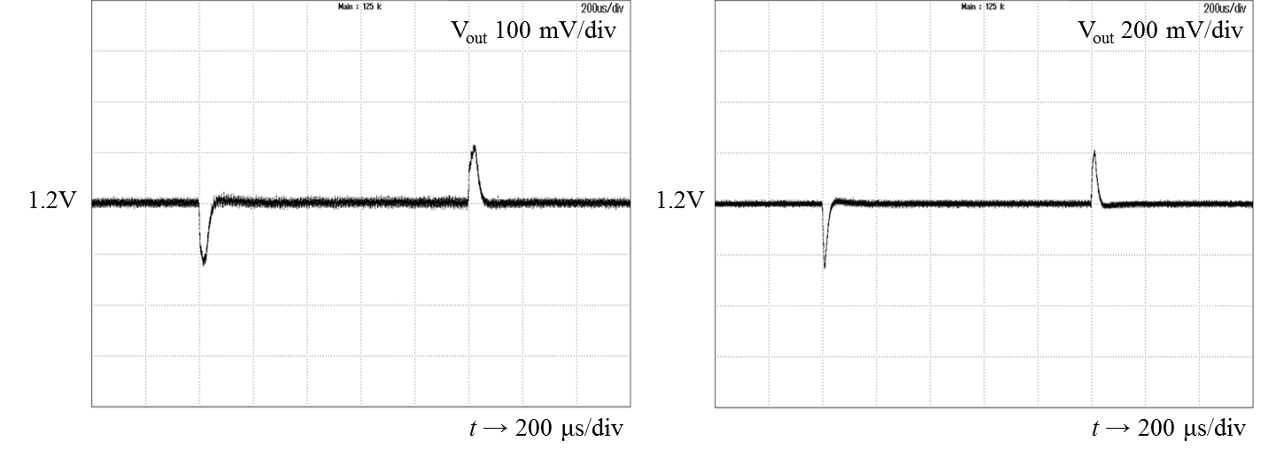
Latest digital control enables ultra-fast response. Compared to the BDP series using previous digital control, voltage change during response has been reduced to half.
Load Response Waveform – BDP (Vin=12V, Vout=1.2V, Iout=0~150A, SR=5A/us)
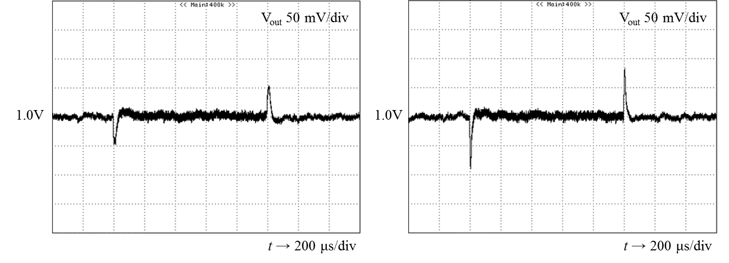
Load Response Waveform – BDP (Vin=12V, Vout=1.0V, Iout=0~100A, SR=5A/us)
As the progress of the minuteness of the process rule for advanced device such as FPGA and ASSP, the requirement on power supply is also going toward low voltage and large current.
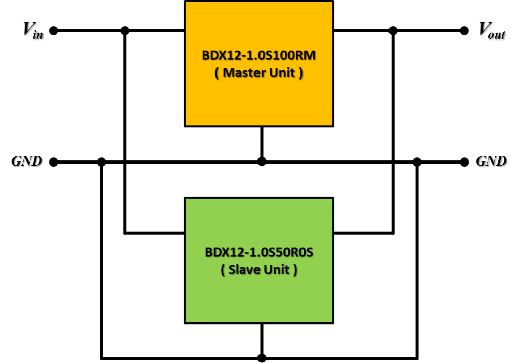
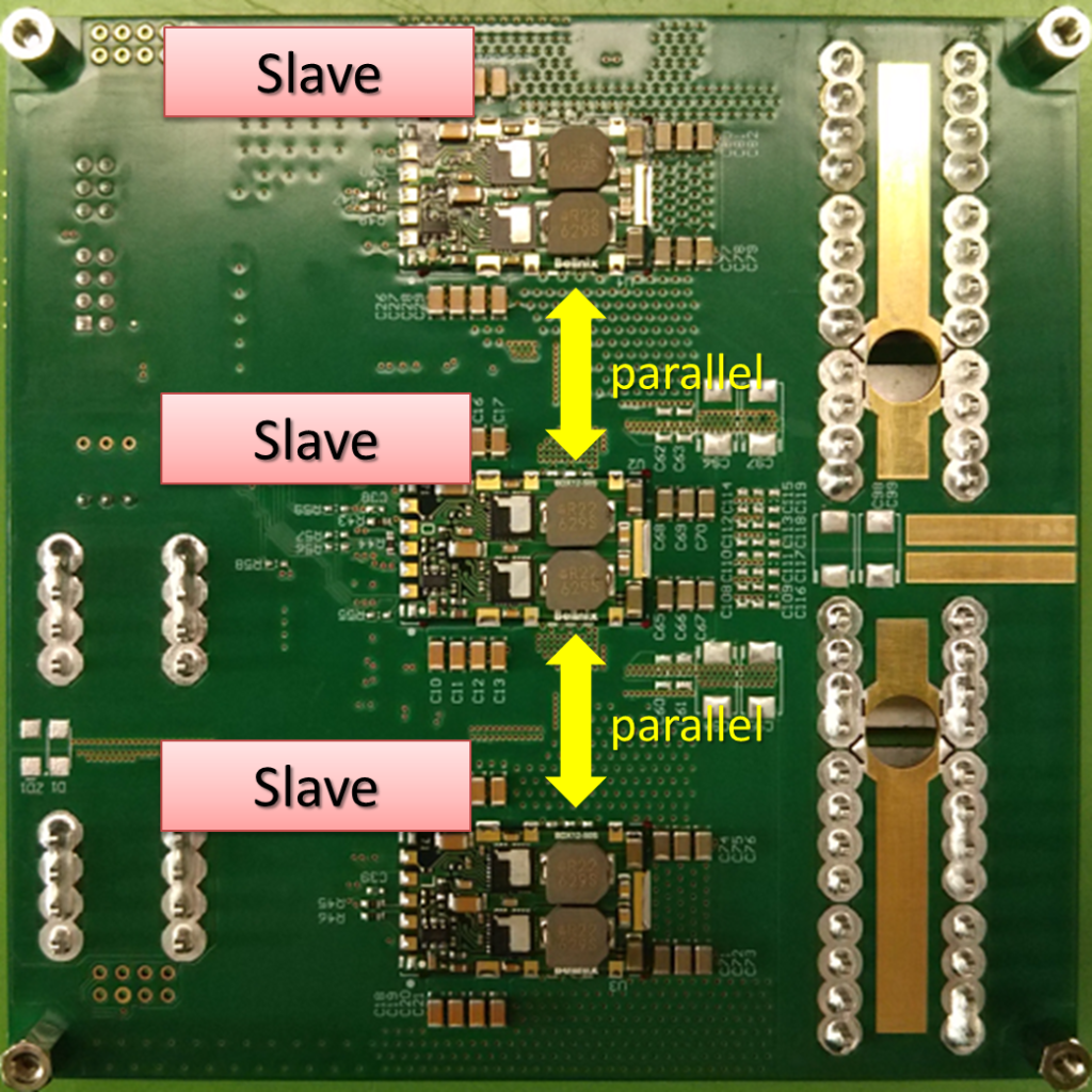
The BDX series features parallel operation enables the power-up on the output current (derating required). Capable to supply up to 350A by connecting 5 slaves at maximum in parallel with one master.
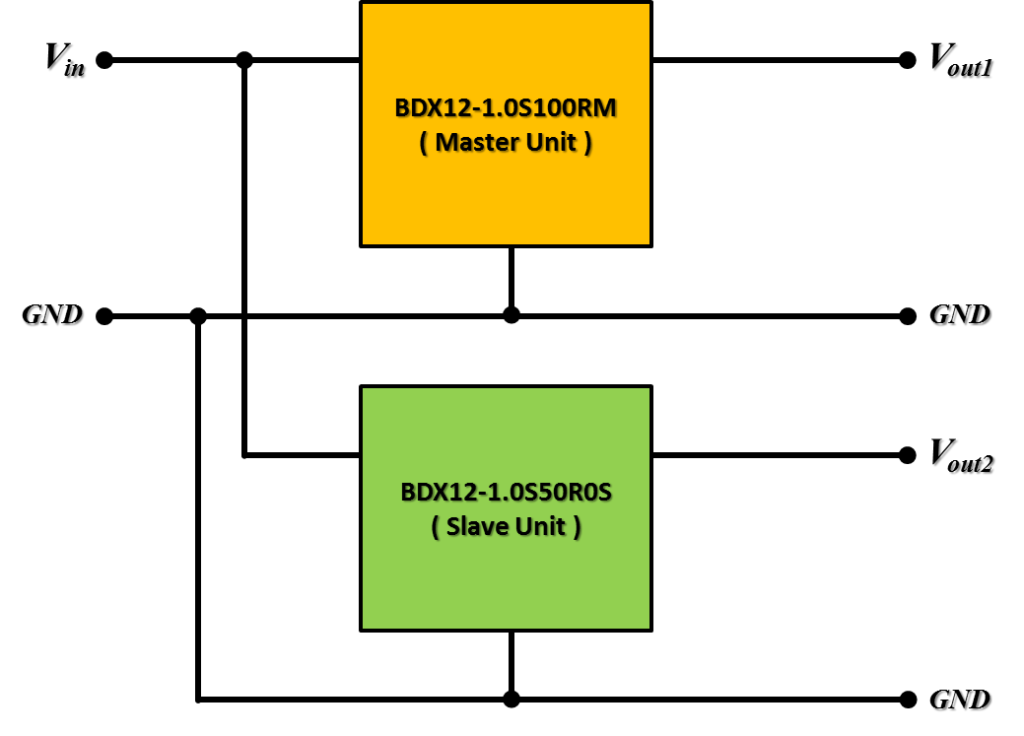
It is also possible to use separately without connecting the outputs to each other.
The VIN, PGND and VOUT pins of BDX12-1.0S100RM and BDX12-1.0S50R0S are designed to be line-symmetric for easy parallel connection, allowing for mounting both sides on PCB.
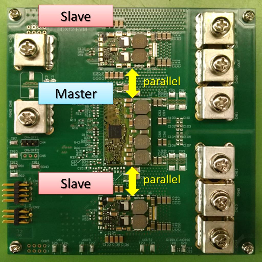
The layout of the evaluation board (BDX12-EVM) for the BDX series is shown below. 5 slaves are placed with master. Each unit is connected in parallel on Top side and on the Bottom.
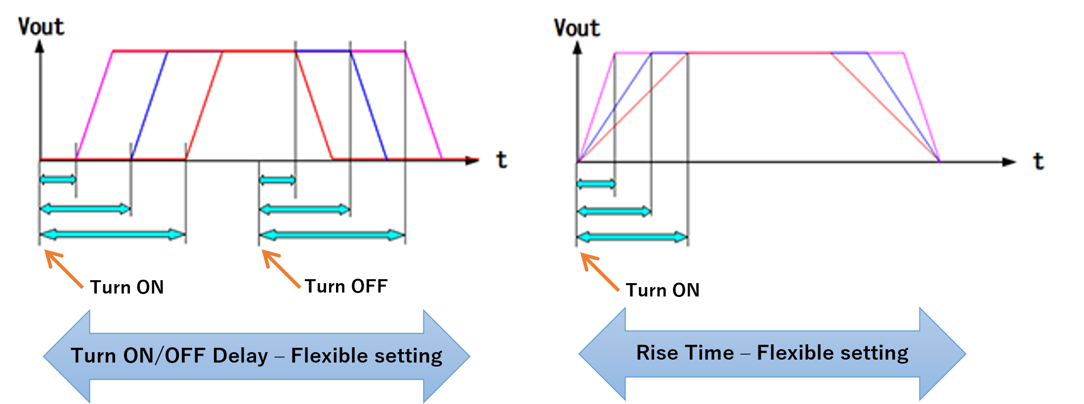
Output voltage, startup time, and rise time can be set and saved with no external components.